
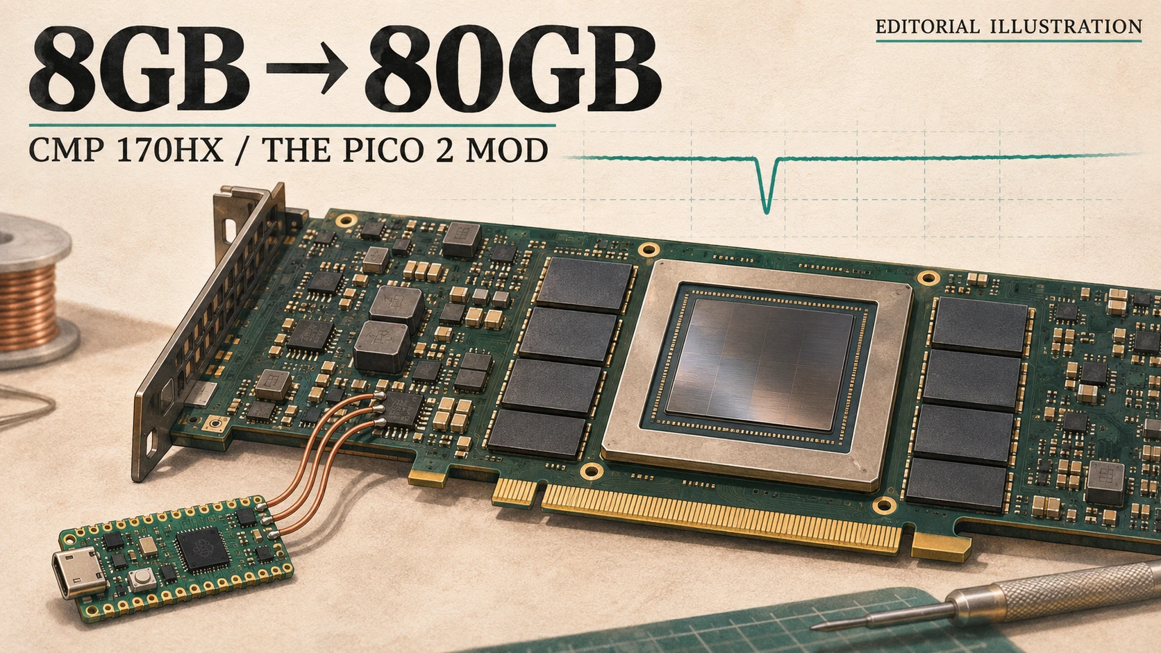
Four fine wires, a Raspberry Pi Pico 2 and a mining card that suddenly reports 80GB of memory. That was the result posted by Reddit user Yarukiless-cat on November 15, after roughly fifteen hours spent reproducing a voltage-glitch attack on NVIDIA's CMP 170HX. The card had started life with just 8GB exposed to applications. The user also reported 126 streaming multiprocessors, opening up far more compute hardware than the mining specification allowed. The original post is brief, but the engineering behind it is anything but.
The small board in this story deserves its full name: Raspberry Pi Pico 2. It is an RP2350 microcontroller board, sold from $5, rather than a Raspberry Pi 5 running Linux. Its job is to control electrical events at the right moment. It supplies neither the extra memory nor the GPU's computing power. Raspberry Pi's Pico 2 specifications describe a device built for embedded control, which is precisely why it fits this experiment.
The memory was already in the package
The CMP 170HX uses GA100 silicon, the same underlying GPU family as the A100. HBM sits beside the GPU die on the package; this is not a modification in which someone solders larger memory chips around the board. The challenge is getting the chip to expose memory and compute blocks that its configuration has disabled.
There were already useful results before the Pico appeared. The cmpunlocker project uses a software path through NVIDIA's Falcon machinery and modified open kernel modules to change memory geometry and compute restrictions. Its established profiles distinguish the 8GB card, commonly taken to 64GB, from the 10GB card, commonly taken to 40GB. Those are different hardware populations. A larger stock memory number does not automatically mean a larger unlocked capacity.
Memory geometry tells the controller how to address the resources available to it. A disabled hardware partition is a different obstacle. Enlarging an address map cannot make an inaccessible partition respond correctly. That distinction explains why the earlier software result and the new 80GB result belong to different chapters of the story.
On November 10, researcher Kate published a hardware route through GA100's fuse controller. Her original rig used an STM32-based board to intercept PWMVID, the signal that tells the voltage regulator what output to produce. A carefully timed voltage disturbance changed how the GPU sensed its security configuration during startup, opening a path to permanent fuse programming. Kate reported 80GiB usable on nine of ten examined cards; one remained limited to 64GiB. This is the research the later Pico implementation builds on.
What the Pico actually changes
The pico-ga100vfi project takes a different route into the same power system. It talks over I2C, using PMBus commands to the card's MP2888B voltage controller. The required connections are ground, SDA, SCL and the GPU's PEX_RST reset signal. The reset release provides the timing reference. The regulator then produces a short dip on NVVDD, the GPU core supply, during the fuse-sensing window.
That arrangement is more interesting than the phrase “a Raspberry Pi unlocks a GPU” suggests. The Pico does not force the rail down by supplying or sinking the GPU's full current. It instructs the regulator already designed to handle that current. The host computer communicates with the Pico over USB and examines the GPU through PCIe BAR0, its register-access window. Timing-sensitive control stays on the microcontroller; inspection and decision-making happen on the host.
The project's build notes describe firmware built with the Pico SDK and installed as a UF2 image through BOOTSEL. They also separate the normal firmware from the diagnostic build that samples the voltage rail. Those samples help explain an attempt; they are not what triggers it. The reset connection is driven low and then released, rather than actively driven high into the GPU's lower-voltage reset circuitry.
In practical terms, the modification has several distinct jobs. Establish communication with the regulator. Synchronize the voltage disturbance to reset. Read back the GPU's state. Find a state that allows the required configuration work. Then, separately, program the appropriate fuse records and bring the card up with software that knows about the newly available resources. A successful voltage glitch is an intermediate result, not an 80GB memory test.
A successful glitch leaves most of the chip working
Simply collapsing the supply is no use. If the GPU reads its entire fuse configuration as zero, it can lose the information needed to initialize correctly. The useful result is narrower: security-related controls become permissive while the remaining configuration still parses.
The Pico protocol documentation calls this the Goldilocks state. It checks for software override being available, a valid fuse CRC and open privilege masks. Its published hardware experiment used a shallow sequence of three pulses rather than one large drop. The host waits for the firmware's completion response before inspecting BAR0. The firmware also has to restore normal regulator control after the attempt. That last operation matters as much as the dip: the board must return to ordinary power management before useful work can begin.
The difference between the voltage command and the voltage at the die is where much of the debugging lives. The bus takes time to transmit a command, the regulator has a response curve, and the board itself adds capacitance and electrical variation. Copying a delay from another card does not copy its power rail.
The project's adaptive calibration notes show the search becoming more systematic. Each attempt is classified, and subsequent voltage choices use those outcomes. An insufficient disturbance leaves override locked; an excessive one can corrupt the configuration read or lose the PCIe link. A recorded November 16 run reached the desired state on attempt eight, in 3.2 seconds. That measures one calibration run on one setup, not the time needed to complete a card conversion.
Why blowing more fuses can enable more hardware
The surprising part is what happens after access is obtained. GA100 has configuration entries known as fuseless fuses. The controller replays a sequence of records; when a later record addresses the same block, its value takes precedence. Appending a new record can therefore change an effective disable mask without physically repairing a previously blown fuse. Kate's write-up explains how this makes previously inaccessible blocks available while retaining masks for known defects.
That is a permanent change to one-time-programmable storage. There is no ordinary firmware rollback for a bad fuse burn. It is also why “all disabled units” and “all good units” are not interchangeable descriptions. The silicon still has to work.
For anyone evaluating the result, the useful evidence starts after the capacity counter changes. A memory test should write across the newly exposed address range and read the data back, with cache effects accounted for. A real workload then adds a different kind of pressure: memory traffic, sustained power draw, temperature and repeated kernel execution. A card that enumerates successfully has passed its first test, not its last.
The attraction for local AI is easy to understand. Model weights alone need roughly two bytes per parameter at 16-bit precision, before runtime buffers and the attention cache enter the picture. A hypothetical 30-billion-parameter model therefore starts at about 60GB of decimal weight storage in that format. Quantization changes the arithmetic, but the basic constraint remains: fitting a workload in local GPU memory can matter more than another small increase in peak arithmetic throughput. Going from 8GB to 80GB changes which workloads are even possible.
From a glitch controller to a Linux workbench
The Pico story also shows why there is room for more than one kind of small board on an engineering bench. The microcontroller handles repeatable electrical timing. A Linux computer stores logs, builds firmware, hosts a dashboard and coordinates instruments. The PCIe host runs the GPU and its driver. Sometimes one machine fills several of those roles; there is no requirement that it do so.
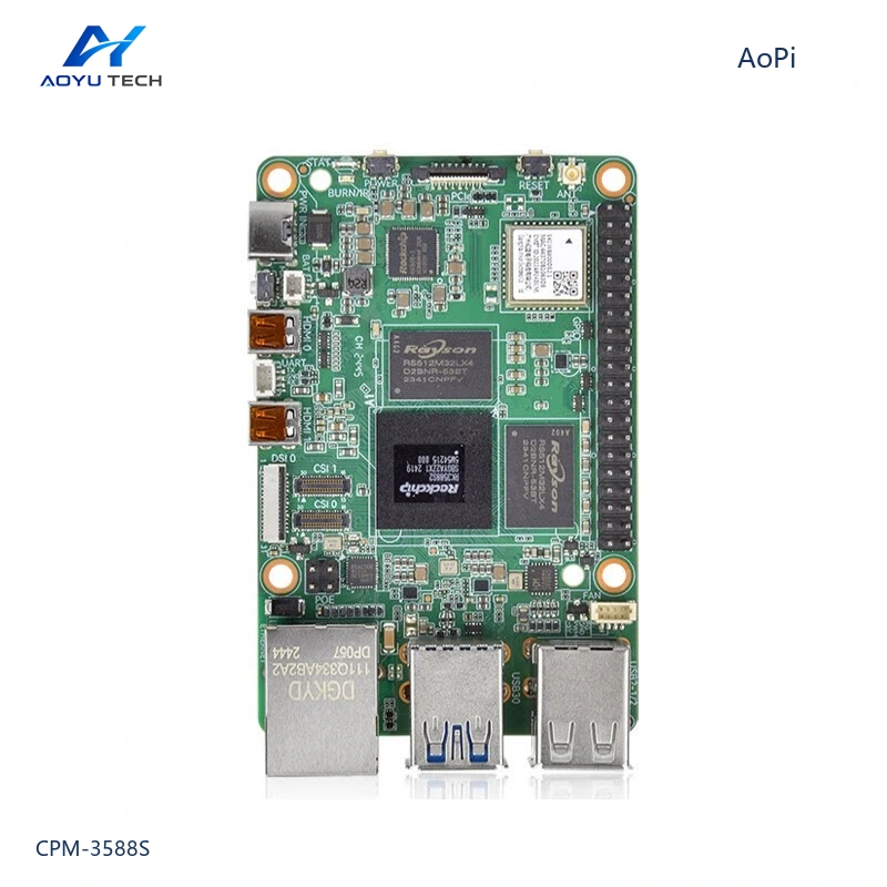
This is where our AoPi CPM-3588S enters the discussion. It belongs alongside Raspberry Pi 5 in the Linux single-board-computer category. AoPi uses the same general board structure as Pi 5, giving it a familiar starting point for compact systems. That mechanical familiarity does not make Raspberry Pi firmware, pin assignments or accessories automatically interchangeable.
AoPi is not being presented here as the board used in the published GPU unlock. Its appeal is in the work around the experiment: a compact engineering console, a data-collection computer, or an embedded system that must combine a local interface with inference and device control.
AoPi 3588S: more integration on the board
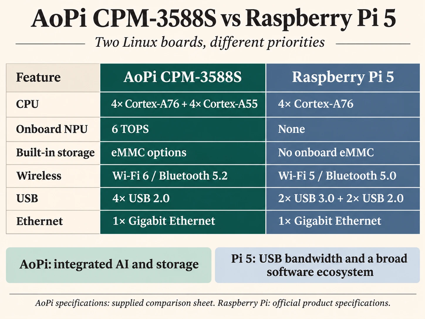
The RK3588S combines four Cortex-A76 cores with four Cortex-A55 cores. The supplied CPM-3588S specification lists clocks up to 2.4GHz and 1.8GHz respectively, alongside a 6 TOPS NPU. The extra small cores give background services somewhere to run while the larger cores handle heavier work. Eight cores do not imply twice the speed of a four-core board; the useful gain depends on how the application divides its work.
The integrated NPU is a more distinctive feature. A camera application can use a supported, converted model for local inference while the CPU handles capture, networking and the user interface. Rockchip's RKNN toolkit provides the model-conversion and deployment path for RK3588-series NPUs. The practical question is whether the model's operators, precision and input pipeline fit that path. The 6 TOPS figure describes the accelerator's rated capability, not a promised frame rate and certainly not CUDA compatibility.
Onboard eMMC is another useful difference. Our current product page lists 4GB RAM with 32GB storage, 8GB with 64GB, and 16GB with 128GB. For a device that must boot into the same interface every morning, having the system storage on the board makes assembly and image deployment simpler. Logs, application packages and local model files also have somewhere to live without occupying a USB port.
The supplied comparison adds Wi-Fi 6, Bluetooth 5.2, Gigabit Ethernet, six UART resources plus a TTL debug serial port, and a 40-pin header. Serial availability is valuable in a fixture or control cabinet: a console, a sensor interface and an external controller may all need separate channels. The connector routing and pin multiplexing determine which functions can be used together. Those are board-integration questions, rather than a reason to count every UART as an already fitted industrial serial socket.
Where Raspberry Pi 5 keeps an advantage
Raspberry Pi 5 has four Cortex-A76 cores at 2.4GHz, two USB 3.0 ports and two USB 2.0 ports. The supplied AoPi sheet specifies four USB 2.0 ports. For an external SSD or a high-bandwidth USB capture device, that difference can outweigh the extra CPU cores. Both boards offer Gigabit Ethernet; AoPi's newer wireless specification does not change the speed of that wired connection.
Pi 5 also brings a well-established operating system, official documentation and a wide accessory ecosystem. For an engineer adapting an existing Pi project, familiar software can save more time than a faster component. It has two four-lane MIPI camera/display transceivers, dual 4K60 HDMI output and a PCIe 2.0 x1 interface. It has no onboard eMMC or NPU; storage and AI acceleration can instead be added through external hardware.
The two boards consequently make different trade-offs. AoPi puts eMMC, an NPU and a mixed eight-core CPU into a familiar compact layout, with Android and Linux listed on our product page. Pi 5 supplies faster native USB connections and a broad base of existing software and peripherals. A vision terminal with local inference has different priorities from a USB-heavy test station.
And neither should be confused with the Pico 2 soldered to the mining card. In the CMP 170HX experiment, the small controller's achievement was exact electrical control. In an AoPi system, the opportunity is to keep the surrounding application compact: capture the data, process it locally, display the result and talk to the equipment. The GPU story is a striking reminder of how much useful engineering starts at the interfaces between chips.
Explore AoPi CPM-3588S configurations and project enquiries →
Related products
Explore our HMI panels
Ready to start your HMI project?
Our engineers help you choose the right HMI hardware and software for your project.